


Telecommunication
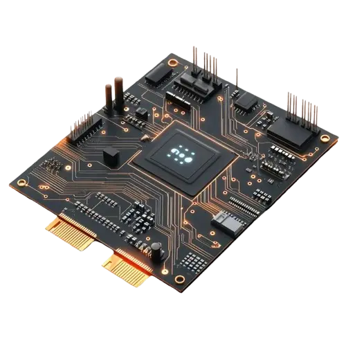
We can design 1.6T Ethernet Switch ASICs and 5G/6G baseband accelerators. It helps the team implement high-speed 22.4G SerDes and DPS to manage massive throughput with ultra-low latency in next-generation network infrastructures
Read More >
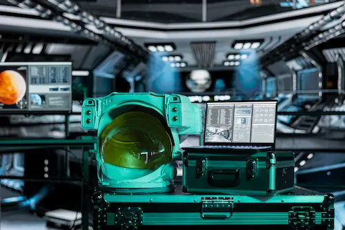
Aerospace
Developing Rad-Hardened ASICs with Triple Modular Redundancy (TMR) for satellite payloads ensures mission critical reliability and SEU-resilience in extreme orbital environments. All of this happens due to high-reliability design flows and the essential toolkit used by Netiqate specialists.
Read More >
Their expertise in the 2nm FinFET node transition was pivotal. We achieved timing closure on our AI accelerator weeks ahead of schedule.
Marcus ThroneChief Architect at Silicon Mexus 
GDSII delivery and UVM-based verification of the firm impressed me a lot. They ensure a perfect first-pass success prototype for the ASIC reference layout in minimal time.
Elena Vance VP of Engineering Quantum Logic 
The Most Reliable team for rad-hardened ASIC design! Their SEU mitigation strategies provided the mission-critical stability our satellite payload required.
Julian RossLead Hardware Engineer at OrbitX Systems